Saw Bench Synth DIY Manual
[dkpdf-button]
Prerequisites
- Soldering iron (nothing too special, any cheap-ass iron will do)
- Soldering tin
- Dupont wire (to hook up panel mount connectors)
- Diagonal cutters for cutting away all the legs of soldered components
- Soldering wick or solder sucker in case of screw-ups
- Philips screwdriver (for M3 screws)
- Multimeter to measure resistors and capacitor values, check for connections and shorts
- Optional: oscilloscope to check presence of digital (MIDI/clocks/PWMs) and analog signals (CV’s, audio)
Tutorials on soldering basics:
Adafruit soldering tools guide
And there are countless others. It’s probably best to study these before you continue..
Also, be aware that the community can help you out: Tasty Chips Forum
Overview
As you may have noticed there are two PCB’s: Analog and Digital. The two are sandwiched on top of eachother (the digital on top of the analog). Analog takes care of power regulation and the signal path (VCO->VCF->VCA) and digital takes care of all controls. Finally there are off-board interfaces like DC power, MIDI, and audio out which will be panel-mounted into the back side of the casing.
Here’s how we proceed through the DIY guide:
- Digital PCB soldering.
- Analog PCB soldering.
- Electrical test.
- Putting it all together (also includes the assembly of the casing).
We’ll cover digital (1) first, because it’s easy enough. Analog (2) involves the same techniques, but it’s more work. So this comes second. Finally (3) there’s how to make the sandwich and put it all into the casing.
Components contained in the electronics kit (aka “bare bones” kit)
Just a quick but precise overview. For details on how the components look or what they do, see further on in this manual.
- 1 bag of capacitors (ceramic, boxcap, elco)
- 22p ceramic 2x
- 100n ceramic 11x
- 100n boxcap 3x
- 220n ceramic 1x
- 330n ceramic 2x
- 330n boxcap 4x
- 1u ceramic 4x
- 1u elco 1x
- 10u elco 1x
- 1 bag of metal film resistors (1%) and diodes
- 1n4148 diode 10x
- 1n4004 diode 1x
- 100R 3x
- 220R 1x
- 470R 2x
- 3k 1x
- 3k9 1x
- 10k 13x
- 12k 9x
- 22k 2x
- 33k 7x
- 100k 7x
- 150k 1x
- 220k 5x
- 1M 2x
- 1 bag of leds, switches and buttons
- 3mm clear blue led, 1500mcd 8x
- push button HIGHLYWELL KS01 B BLUE 2x
- toggle switch TSSM1022A1 2x
- 1 bag of potentiometers
- 9mm wide potentiometer, 6mm D shaft, 25mm high, 10k, linear: Bourns PTV09A-4025FB103 6x
- 1 bag of potentiometer knobs
- Sifam 3/03/DR110-006/237/233 6x
- 1 piece of conductive foam with IC’s and IC sockets
- LT1013DP 4x
- 6N137 1x
- 74HC595 1x
- LM13700 1x
- Atmega 328P (flashed with firmware!) 1x
- 8p DIP header 5x
- 16p DIP header 2x
- 28p DIP header 1x
- 1 bag of headers, transistors,fuse and power regulator
- 6pin male header 4x
- 6pin female header 4x
- 2pin male 90 degrees, Molex MX-7395-02B 3x
- 7805 regulator 1x
- 2n3904 transistor 3x
- 2n3906 transistor 3x
- 16 MHz crystal 1x
- SMD 500mA Fuse – slo-blo + Fuse holder (Littelfuse 0154.500DRT) 1x
- panel-mount connectors
- DIN-5 female 1x
- 6.35mm jack 1x
- 2.1 mm jack 1x
- 1 digital board
- 1 analog board Rev 0 (unmarked) or A
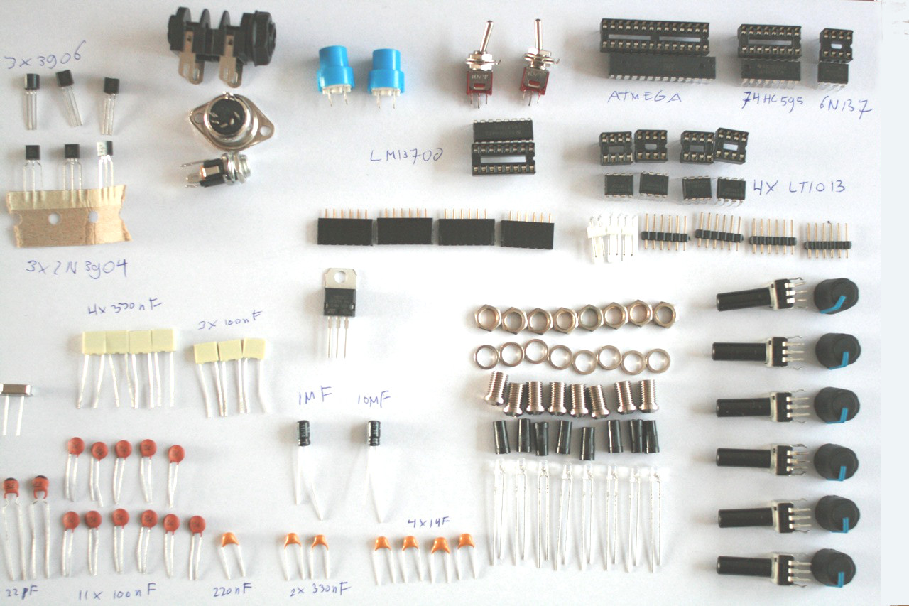
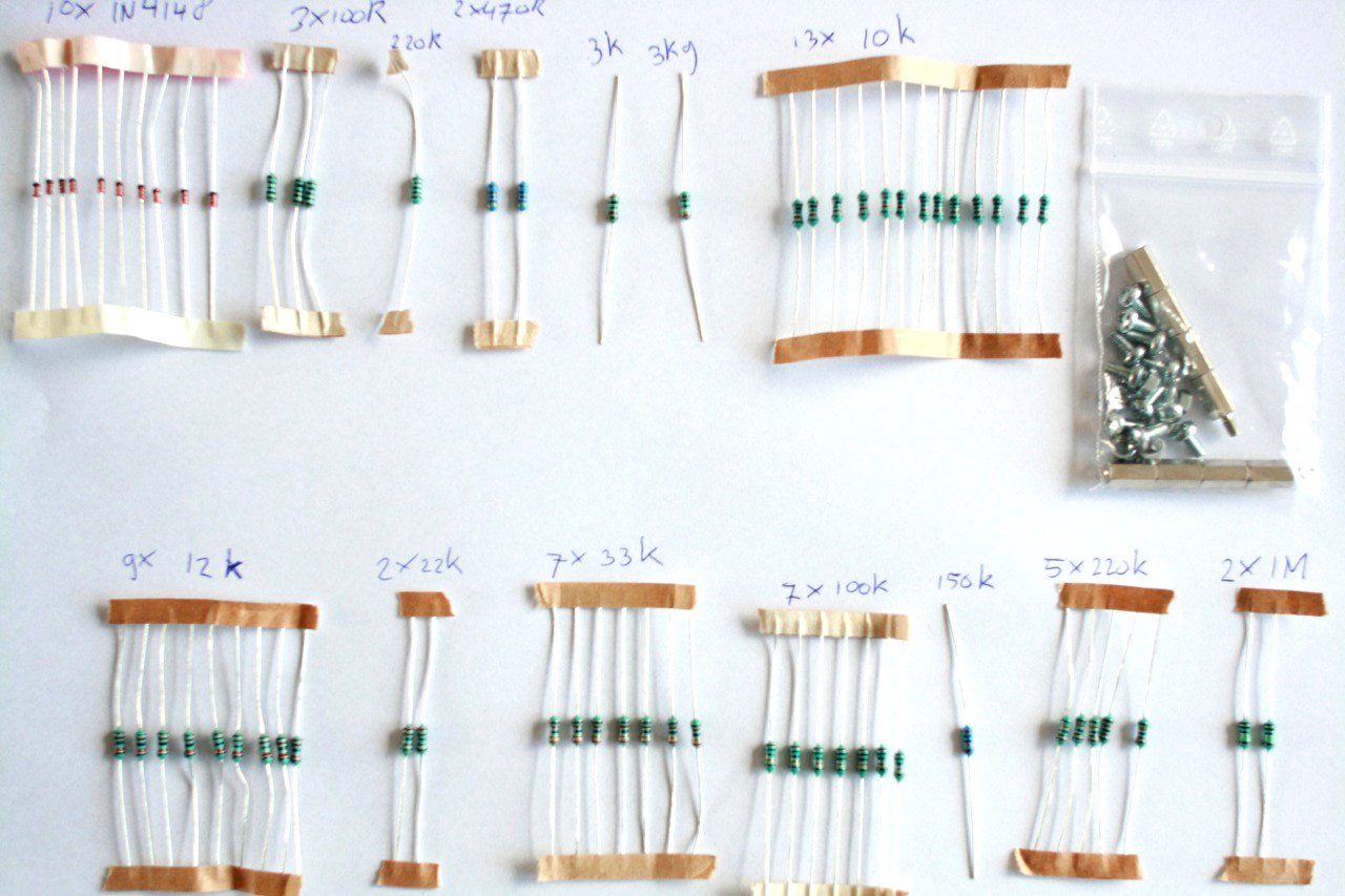
Useful : detailed graphical table of all components:
Useful : photos of all components. Print these and overlay the components to check if they’re all there!
Digital PCB
The digital board is the big board. It houses the microcontroller, all the leds, buttons, switches and potmeters. It also has 2 MIDI input pins for off-board connection.
Resistors (1%, metal film):
220R 1x
3K9 1x
10K 4x
12K 8x
1M 1x
Potentiometers:
B10k 6x
Knobs
Sifam 3/03/DR110-006/237/233 6x
Diodes:
1n4148 1x
3mm LED’s clear blue, 1500 mcd 8x
LED spacers (outer dimension = 4mm, height = 10mm) 8x
LED holders, RTM3010-NI 8x (casing only)
Capacitors:
22 pF 2x
100 nF 6x
220 nF 1x
switches and buttons:
push button HIGHLYWELL KS01 B BLUE 2x
toggle switch TSSM1022A1 2x
crystal:
16 MHz 1x
IC’s:
6N137 DIP 1x
Atmel328p DIP 1x
74HC595 DIP 1x
headers:
6-pin male 4x
2-pin male 1x
Let’s do it!
Typically a PCB is soldered from the bottom up. Why? Because otherwise you’ll block the soldering iron with all those high components, dummy! Maybe you like the smell of burning plastic? Otherwise, just read on. 😉
Diodes
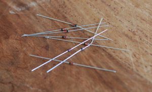
You’ll start with the lowest components: the 1N4148 diodes. These are little 3mm long glass thingies, the smallest components in the kit. There is only 1 of these on the digital board.
ATTENTION: diodes are POLARIZED! They will only work if you place them in the right direction. Reversing them will result in a non-working PCB.
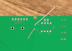
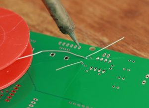
How to solder these? Here’s the 6 step plan to solder diodes and resistors:
- Fold the legs of the diode as closely to the glass as possible, until you have an ‘n’ shape.
- Insert the two legs through the holes. Note the direction! The stripe on the PCB silk screen should align with the stripe on the component! If you fail to do this correctly, the PCB won’t work.
- Push the component all the way down.
- Fold the legs on the bottom side of the PCB.
- Solder the points where the legs enter the PCB holes.
- Cut away the legs. Do this close the PCB, but don’t overdo it, you may snap away the tin.

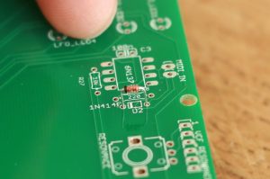

Headers
These are 4 6-pin and 1 2-pin male headers (in newer kits this is a white 90 degrees version, not a straight one!).
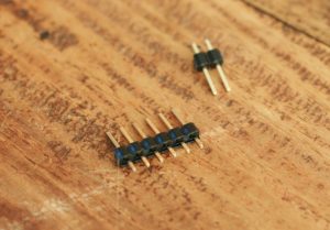
The male headers can just be pushed into the PCB holes and when you lay down the PCB with the header inserted it will stay there. The longest side should stick out of the bottom side. The plastic should also be on the bottom. So, soldering should be done on top top side. Since the header is stuck in the PCB, just proceed and solder all the pins in a row. You’re done with the headers.

Resistors
Next step is the resistors. The resistors are about 6 mm long and somewhat higher than a diode. Resistors are not polarized, so you don’t need to worry about the direction. Resistors are color coded. This means you can read their value by interpreting the coloured bands printed on them.
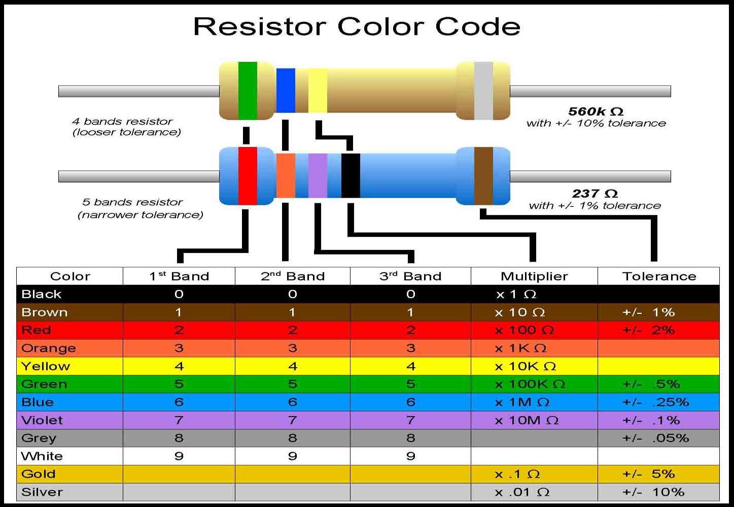 Resistor color codes
Note that you can also measure the resistor value with a multimeter, which is essential to the color blind, but also useful for people with normal eye sight.
Forget the brown one on the top. That’s too inaccurate for us. Look at the blue one, with 5 bands. These puppies are 1% tolerance. Which means at most a 100 ohm resistor could be between 99 and 101 ohm. Good enough.
Looking at the resistor list:
220R 1x
3K9 1x
10K 4x
12K 8x
1M 1x
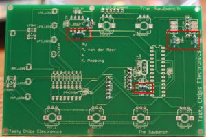
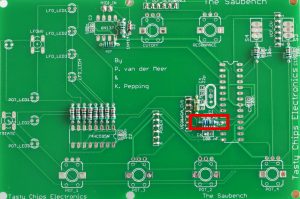
You can see that these are grouped and sorted by value. Solder each group like specified in the 6-step plan above. Look at the pictures below for the positions.



Crystal

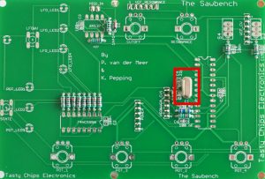
The crystal is found left of the Atmega. Solder it just like any 2 leg component. Use the 6-step plan.
IC sockets

1x DIP8 (for 6N137): OK1
1x DIP16 (for 74HC595): SHIFT_REGISTER_
1x DIP28 (for Atmel328p): U1
Here a 4 step plan to solder these puppies:
- Place the socket over the pins where it belongs. For instance, IC1 has a DIP8. The direction is important here. Position the socket over the silkscreen drawing with the little gap aligned.
- Push down the socket. Or in most cases, just let it slide in. Gravity will do the rest.
- Bend the outer most socket pins to secure the socket.. For instance, the upper-left pin and the lower-right pin.
- Solder all pins on the bottom of the PCB.
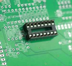

The best way to proceed is to first do steps 1 through 3 for all sockets and then collectively do 4. This speeds things up.

Capacitors
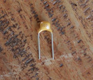
These are the capacitors that have a relatively low form factor: just slightly higher than sockets. The high capacitors (the black cylinders) are special ones, called electrolytic capacitors (or elco’s). These will come later on.
Let’s start with the ceramic disk 100n ones. These have “104” written on them. You can use the 6-step plan, the same as for resistors.

Next up are the 220n droplet (labeled “224”) and 22p (labeled “22”) ceramic capacitors. Once again use the 6-step plan.

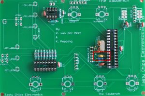
Push buttons:
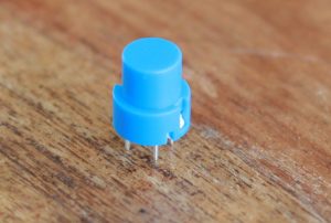
These should be pushed into the PCB with the with the white side along the length direction of the PCB. Sounds a bit hard? Here’s a photo:
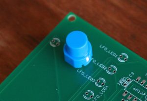
If the button has the wrong orientation (90 or -90 degrees rotated) then it won’t work! Be careful! The buttons are labeled “S1” and “S2” and should be easy enough to find on the PCB.

Switches:

These are symmetric and can be placed any way you want. They are labeled S3 and S4 and are easy to find on the PCB. Some things to keep in mind: you mind want to fasten them while soldering (duct tape? ;)). More importantly: The pads are pretty big and invite you to smack a big lump of solder on them. Unfortunately they’re also very close to eachother, so watch out! Don’t use too much tin!

LEDs and spacers:
First of all: the LEDs are part of the electronics kit, the spacers are part of casing. We expect bare bones DIY’ers to fix up their own casing and possibly their own LED housings. What is explained here is intended for usage with the full kit, including the casing!
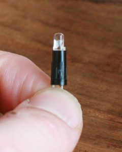
In any case, this is the trickiest part of the digital board! LEDs are polarized. The long leg is + and the short one is -. The long one should go into the hole with the trace. See the pictures. Also, the spacer should have its thin side up, wide side down.

When placed on the PCB, even when you cannot see the leads you can still make out the orientation by looking inside the LED.

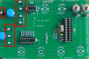
7 out of 8 leds are oriented with the + leg to the right. only the LFO led (the isolated one most to the left) is the other way around. Once again, this is important!!
Potentiometers
The potentiometers are almost trivial: there’s only one type and there’s only one way to fit them. Just push them in. You should feel them “snap” into the PCB. They are now already stuck in place. When all 6 are inside, just flip over the board and solder them.
And finally
That’s it.. just put in all the IC’s.. (with the correct orientation: mind the side of the gaps and the dots) and that’s it 🙂
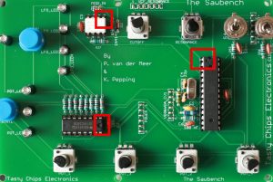
The analog board is the small board. It houses all the analog units: VCO, VCA, VCF and power regulation. The analog is sandwiched underneath the digital board from which it receives control voltages. Sandwiching is done with 6 pin headers. Off-board connections are two 2-pin male headers: power and audio out.
ATTENTION:
There are two revisions of the analog PCB, 0 and A. Rev A is the current revision being shipped as of October 2016. It is marked on the silkscreen of the PCB’s. There is no difference in performance. The only difference is that we added a protection diode and fuse. This will protect the circuitry from accidentally reversing the polarity!
Components
For pictures, see below.
Resistors (1%, metal film):
100R 3x
470R 2x
3k 1x
10k 9x
12k 1x
22k 2x
33k 7x
100k 7x
150k 1x
220k 5x
1M 1x
Diodes:
1n4148 9x
1n4004 1x
Transistors:
2n3906 3x
2n3904 3x
Capacitors:
ceramic:
100n 5x
330n 2x
1u 4x
polyester film:
100n 3x
330n 4x
elco:
1 uF, Yageo SS050M1R00-0407 1x
10 uF, Yageo SS050M0010-0407 1x
Fuse:
SMD 500mA Fuse – slo-blo + Fuse holder (Littelfuse 0154.500DRT) 1x
IC’s:
LM13700 1x
LT1013 4x
7805 TO220 1x
IC sockets:
DIP8 4x
DIP16 1x
headers:
female 6pin 4x
90 degree male 2pin Molex MX-7395-02B 2x
Let’s do it!
Typically a PCB is soldered from the bottom up. Why? Because otherwise you’ll block the soldering iron with all those high components, dummy! Maybe you like the smell of burning plastic? Otherwise, just read on. 😉
Diodes

You’ll start with the lowest components: the 1N4148 diodes. These are little 3mm long glass thingies, the smallest components in the kit. There are 9 of these on the analog board. 8 of them are in the VCF, in one large column. The remaining one is in the VCO.
ATTENTION: diodes are POLARIZED! They will only work if you place them in the right direction. Reversing them will result in a non-working PCB.
How to solder these? Here’s the 6 step plan to solder diodes and resistors:
- Fold the legs of the diode as closely to the glass as possible, until you have an ‘n’ shape.
- Insert the two legs through the holes. Note the direction! The stripe on the PCB silk screen should align with the stripe on the component! If you fail to do this correctly, the PCB won’t work.
- Push the component all the way down.
- Fold the legs on the bottom side of the PCB.
- Solder the points where the legs enter the PCB holes.
- Cut away the legs. Do this close the PCB, but don’t overdo it, you may snap away the tin.
It’s probably best to perform steps 1 to 5 for all the diodes and only then proceed to 6. It saves time.
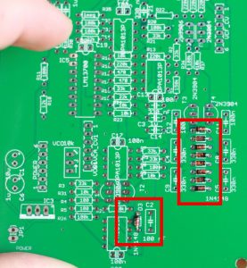
Resistors
Next step is the resistors. The resistors are about 6 mm long and somewhat higher than a diode. Resistors are not polarized, so you don’t need to worry about the direction. Resistors are color coded. This means you can read their value by interpreting the coloured bands printed on them.
 Resistor color codes
Note that you can also measure the resistor value with a multimeter, which is essential to the color blind, but also useful for people with normal eye sight.
Forget the brown one on the top. That’s too inaccurate for us. Look at the blue one, with 5 bands. These puppies are 1% tolerance. Which means at most a 100 ohm resistor could be between 99 and 101 ohm. Good enough.
Looking at the resistor list:
100R 3x
470R 2x
10k 9x
12k 1x
22k 2x
33k 7x
100k 7x
150k 1x
220k 5x
1M 1x
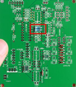
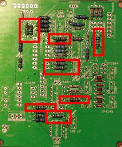
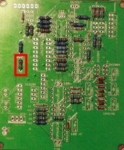
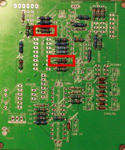
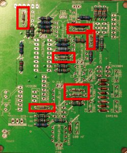
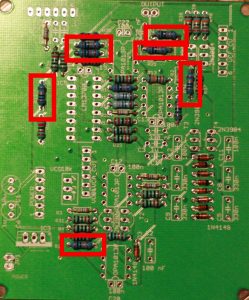
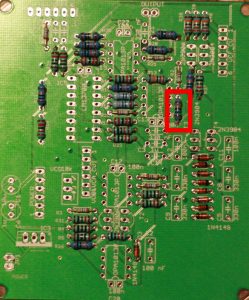
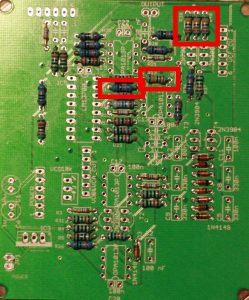
You can see that these are grouped and sorted by value. Solder each group like specified in the 6-step plan above. Look at the pictures below for the positions.

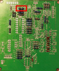
IC sockets

1x DIP16 (for LM13700): IC5
4x DIP8 (for LT1013): IC1, IC2, IC4, VCFIC
Here a 4 step plan to solder these puppies:
- Place the socket over the pins where it belongs. For instance, IC1 has a DIP8. The direction is important here. Position the socket over the silkscreen drawing with the little gap aligned.
- Push down the socket. Or in most cases, just let it slide in. Gravity will do the rest.
- Bend the outer most socket pins to secure the socket.. For instance, the upper-left pin and the lower-right pin.
- Solder all pins on the bottom of the PCB.


The best way to proceed is to first do steps 1 through 3 for all sockets and then collectively do 4. This speeds things up.
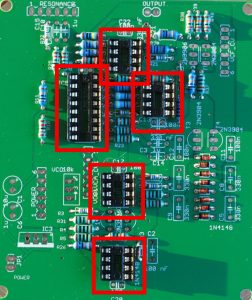
Ceramic capacitors

These are the capacitors that have a relatively low form factor: just slightly higher than sockets. The high capacitors (the black cylinders) are special ones, called electrolytic capacitors (or elco’s). These will come later on.
100n 5x
330n 2x
1u 4x
Let’s start with the ceramic disk 100n ones, marked “104”. These are used to avoid noise and spikes on the IC’s. TODO: component picture You can use the 6-step plan, the same as for resistors.
Next up are the 330n droplet and 1u ceramic capacitors. TODO: component piccy. Once again use the 6-step plan. The value is written on them: “105” means 1uF, “334” means 330 nF.


Transistors

These are three-legged black thingies. We’re using the types “3904” and “3906” here, which is also written on them. But the writing is pretty small and since three digits are the same it sometimes requires you squinting your eyes, or installing better lighting to distinguish between the two. This is essential, the circuit will not work when the two types are swapped. Also keep in mind that the transistors should be aligned like on the silkscreen. The round and flat sides should align. It’s probably best to first solder one kind and then solder the other. The 3904 is used in the VCF 3 times, and the 3 3906 is used in the VCO twice and once in the VCF.


Polyester film capacitors
Now the polyester film caps.

100n 3x
330n 4x
These are capacitors that are not easily influenced by temperature and hence are ideal for VCO and VCF. They are shaped like a flat box. 4x 330n and 2x 100n go into the VCF. They are present in two columns. 1x 100n goes into the VCO.


Trimmer (trim pot)
The trim potentiometer was used in the prototype design, it may still be useful for when modding the saw bench, but the newer firmwares do not need it. A 3k (or 2k7 or 3k3) resistor can be placed between terminals 1 and 2 instead (check the silkscreen: these are terminals furthest away from the drawing of the screw).

Elco’s (Electrolytic capacitors)
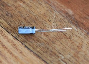
There are only two of these and they are part of power regulation. Note that these are POLARIZED! Reversing the leads will result in the destruction of the elco! The elco’s top will start to bulge, which is an indication that it is ruined! The negative lead is shorter than the positive lead and also the negative side is indicated on the cylinder by a white stripe. The elco’s supplied in the kit are special low-profile ones. There are many types which do not fit in the sandwich!! The DIY buyer beware!

IC’s
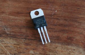
Only the 7805 needs soldering here, the other IC’s just go into their sockets. The 7805 is located on the lower left side of the PCB. This regulates the incoming DC voltage (9V .. 12V) back down to a stable 5V. It’s the big 3 legged thing. This thing is polarized, but the silkscreen is very clear about what back and front should be. This component can be soldered on top. When you’re done, cut the excess leads and bend the 7805 back towards the edge of the board.
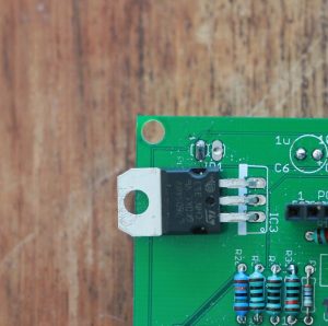
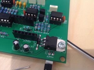
Push IC’s IC1, IC2, IC4, IC5 and ICVCF into their respective IC sockets. Take care of the orientation. For the LM13700: the little gap on the silkscreen should match the one on the IC. For the LT1013’s: the dot on the IC should be on the side of the silkscreen gap. Once again, orientation is important here. Reverse it and the IC’s may get fried!!
ATTENTION:
The following steps are only required if you have Revision A of the Analog Board. You can check this on the silkscreen or look for two SMD pads on the bottom side of the PCB
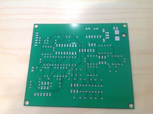
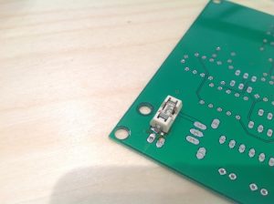
In the new revision we added a fuse to protect the board. It is mounted on the bottom side of the PCB. As you can see in the picture above the fuse goes on the big shiny SMD pads underneath the 7805 regulator
Protection Diode
Beside the fuse we added a 1n4004 protection diode. It goes on the component side of the PCB. This is a POLARIZED component so watch for the marking on the silkscreen. When the polarity is accidentally reversed the current will flow through the diode breaking the fuse.

Headers

There are 4 6-pin stackable headers. Just place one through the holes, don’t bend the pins, keep it pushed down, and solder the first pin. You can also turn the board upside-down with the header in place. Then you’ll have both hands free. 😉 Solder the pins. Repeat for the other 3.
There are two 2-pin male headers for power in (labeled “JP1” / “POWER”) and audio out (labeled “OUTPUT”).
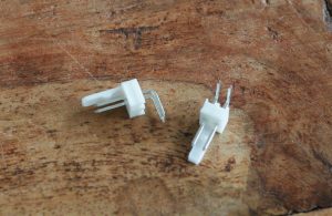
Push in the 90 degree male headers. The longest side should stick out of the bottom side. You can use tape to keep em there. Or you can use your hands if you’re just a bit more handy. Then just solder all the pins and you’re done.

You’re done with the analog board! Loads of different types of components, but it all ended well, didn’t it?


Putting it all together
Panel mount connectors
2.1 mm DC supply socket, wired 1x
DIN-5 socket, wired 1x
phono 6.35mm jack (CLIFF CL1160A), wired 1x
First to solder the wires to the connectors. Easiest is to use dupont female-to-male wires for this. Solder the male side to the connectors and fit the female side onto the headers. See the picture below for instructions on which pin is which.
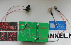
Everything is soldered, and the Sawbench should basically work. A quick electrical test is good idea.
1) Hook up audio out. (This is a line output, it cannot drive a headphone!)
2) Hook up MIDI in (make sure the right MIDI channel is used in your setup, the default is 1).
3) Hook up power. Look at the manual: this should be 9-12V DC, center positive and at least 1A. If rated current is too low the sawbench will be half functional and will give off a nasty mains hum.
4) A short start-up sequence should be visible. The LEDs should start scrolling faster and faster and finally the LFO LED should start pulsing. This means there is power and the microcontroller is functional.
5) Test the blue buttons: pressing them should scroll through the LEDs.
6) Try playing a note. Cutoff should be open, VCA Attack and Decay should be 0, Sustain should be completely open. If you hear the note playing: congratulations!
7) Try the toggles and pots to test if the control components are correctly soldered.
Troubleshooting:
Check list:
1. Is 5V present on the atmels and 595’s supply pins?
2. Is the startup sequence: blinking leds, showing?
3. Is there a signal on the 6n137 pin 6 when MIDI data is playing?
The most common mistakes:
– Reversed components. When the Atmel is reversed the LEDs won’t light up! Same goes for reversal of the 595. A reversed opamp is a dead opamp.
– Reversed MIDI or power wires..
– Bad contacts. Be sure to double check all contacts. For the digital board it’s simple. A bad contact on the microcontroller means a completely non-working synth. For the analog board it’s more complicated. For instance, a bad contact in the VCF may increase the cutoff frequency. It won’t hurt to resolder all of the points on the analog board.
Contents of the casing kit
- casing 1x (including anti-slip pads)
- front plate 1x
- M3 spacers, 10 mm high 8x
- M3 nut 6x
- M3 philips cheese head screw 12x
- LED housing RTM-3010-NI (housing, spacer/plug, nut, ring) 8x
Not included but recommended for optimal fastening (involves crimping of ferrules):
- Molex MX-6471-021 2pin female header 3x (for optional friction lock of output and power connectors)
- Molex MX-4809 Female ferrules 6x
Fasten the connectors onto the casing
Assuming the connectors have now been wired (see above).. The MIDI connector is secured with two screws. The screws can be additionally fastened with M3 nuts. The other connectors are fastened screwing on their own nuts.
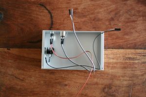
Insert the LED housings into the front plate
The nickel LED housings should be inserted into the frontplate like shown in the photo below. They should be fastened with the supplied nuts. The rings may also be used for a more robust assembly (although our tests revealed that their added value is marginal).
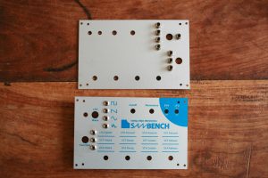
Fasten the electric sandwich
Use the spacers, screws, and nuts to make sure the analog board will never let go. Although the headers are already sufficient the keep the PCB’s stuck toghether this measure will ensure they will stick even when treated very roughly.
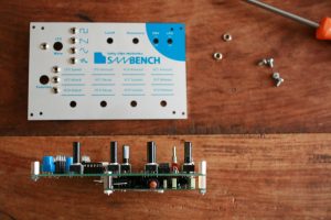
Push electronics into frontplate
For this to work the toggle switches should be cleaned: all the nuts and washers should be gone. And also it goes without saying (well, we’re saying it anyway), that the pot knobs should be removed also.
The frontplate should be slid over all the control elements (toggles, pots, button, LEDs) and then be pushed down gently. Toggles and pots should be easy. LED’s can be tricky because they can be somewhat non-perpendicular to the PCB. The same goes for the buttons. When you push down, you can align the buttons and leds with a screwdriver. Often that works miracles.
Now push down a bit more until the frontplate touches the spacers. The LEDs should also start bulging through the front plate.
When that’s done, screw in the inner screws. This reliably fastens the front plate to the electronics. The nuts can now be screwed onto the toggle switches.
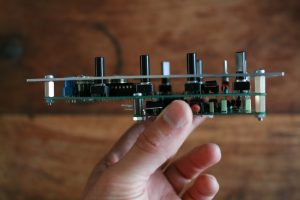
Fasten frontplate and electronics to casing
The final step: just insert the whole frontplate+electronics assembly into the casing.
Make sure you test once more. Power on and play some notes.
Then screw in the outer screws, and presto! The Sawbench is complete!
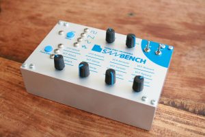
Open source hardware and software
The Sawbench hardware and software is now (Nov 2018) completely open source and in the public domain. You may hack and experiment with the source code and schematics as you see fit.
Open source software on github:
sawbench firmware source code, schematics & layout
step sequencer for Atari ST
The firmware can be hacked and uploaded to a standard Arduino UNO (Atmega328-based). The Atmega from the UNO can then be placed in the Sawbench. There will be firmware updates from us, certainly when bugs need fixing (for instance, the MIDI overflow bug which was fixed in v1.1). And, you can also hack it yourself, for instance to set a different MIDI channel. The firmware on github also contains a readme on how to update the Atmega328.
If your Sawbench is not working and you are out of ideas what could be the problem, you can try the forum or contact us by mail: tastychipselectronics@gmail.com.
Frontplate drills DXF:
DXF file
The drills file is useful if you want to DIY your own casing.

